
-
 Email: admin@ytoptics.com
-
 English Inquiry Support:
-
 Add: 2# Automotive InnovationPark,
City,Jilin Province, China
From Microns to Nanometers: How Optical Components Support the Limits of Precision in Semiconductor
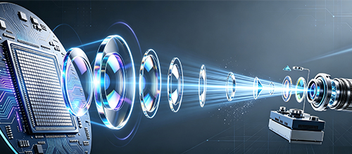
Semiconductor manufacturing is the industrial activity with the most demanding precision requirements to date. As process nodes continue to approach physical limits and feature sizes on chips have shrunk to the nanometer scale, this means that errors in every optical component of the manufacturing process must be controlled within an extremely narrow range. In this race for precision, optical components—lenses, windows, filters, and prisms—play an irreplaceable role; they serve as both the “pen tip” that projects patterns in lithography systems and the “eyes” that enable inspection equipment to identify defects.
The Critical Role of Optical Systems in Semiconductor Manufacturing
Semiconductor manufacturing relies on optical systems in two key areas: lithography and inspection. In the lithography process, the light beam emitted by the light source must pass through a complex optical shaping and homogenization system before being precisely scaled and exposed onto the wafer surface via a projection objective lens. The numerical aperture, level of aberration correction, and transmittance of the optical system directly determine the resolution and overlay accuracy of the lithography system. In the inspection stage—ranging from critical dimension measurement to wafer surface defect detection—the performance of the microscope objective determines how small a defect or how fine a structure the equipment can “see.”
Take the measurement of key dimensions on masks in the deep ultraviolet (DUV) wavelength band as an example: a 248-nm water-immersion objective with a numerical aperture as high as 1.25. Comprising 19 fused quartz and calcium fluoride monolithic lenses, this objective has a total length of only about 72 millimeters. Yet it must achieve near-diffraction-limited imaging quality within a bandwidth of 248 ± 8 nm, while also being compatible with visible-light objectives and a 903-nm laser autofocus module mounted on the same turret. This optical design, subject to multiple constraints, tests the company’s capabilities across the entire supply chain—from material selection to assembly processes.
Technical Depth from Materials to Coatings
The performance limits of semiconductor optical components are primarily determined by the materials used. Fused quartz and calcium fluoride are the materials of choice for DUV optical systems due to their high transmittance and low absorption characteristics in the deep ultraviolet (DUV) wavelength range. In detection applications covering a broader spectral range, the design of wide-spectrum microscopy objectives—spanning from the near-ultraviolet to the near-infrared—requires the use of dispersion vector analysis to guide the selection of glass materials, thereby achieving flat-field apochromatic correction.
Coating technology represents another critical factor in the performance of optical components. Anti-reflection coatings, high-reflectance coatings, bandpass filters, and notch filters—these functional coatings directly determine the signal-to-noise ratio and measurement accuracy of optical systems. Take band-stop filters as an example: they must reflect specific wavelength bands (such as laser excitation lines) while efficiently transmitting all other wavelengths, with an optical density (OD) of 4 or higher. This places extremely high demands on the control of the number of coating layers and thickness precision. Bandpass filters, on the other hand, act as wavelength selectors in fluorescence microscopy, spectrometers, and machine vision inspection; narrow-band products can compress the bandwidth to 2–5 nm.
Machining Precision: A Nanoscale Engineering Challenge
The machining precision of optical components in semiconductor applications has nearly reached the limits of what is physically possible. Surface flatness is measured in λ (633 nm); high-grade products must achieve a flatness of λ/10 and a surface quality of 20/10 according to the scratch-and-pitting standard. For lens elements, this means that every process step—from rough grinding and fine grinding to polishing—must be precisely controlled.
The assembly stage presents an even greater challenge. In the manufacture of DUV microscope objectives, since deep ultraviolet light degrades traditional optical adhesives, the design must employ “air gap” technology, which involves assembling the lenses without any adhesive. This requires that the assembly tolerance of the air gap be controlled within approximately ±2 μm. To achieve this, researchers abandoned the traditional method of securing lenses by rolling the edges of the lens mount and instead used a combination of elastic spacers and clamping rings to secure the lenses, thereby avoiding wavefront distortion caused by asymmetric mechanical stress. This level of assembly precision exceeds the conventional capabilities of most precision machining processes.
A Company with Deep Expertise in Optical Manufacturing
As a manufacturer of semiconductor optical components, Changchun Yutai Optics Co.,Ltd. was established in 2015 and has consistently focused on the research, development, and fabrication of high-performance optical components. Its products are widely used in imaging, defense, medical, and laser applications.
Yutai Optics’ core competency lies in the manufacturing of optical components, with particular expertise in the processing of extra-large, micro-sized, and ultra-high-precision products. Its product line covers six major categories of optical components: lenses, mirrors, beam splitters, filters, prisms, and windows. Material options include BK7, fused quartz, synthetic quartz, B270 heat-resistant glass, and optical glass from major brands.
For users of semiconductor equipment, the “customizability” of optical components is often more critical than the performance parameters of standard products. The optical path structures, working distances, field-of-view requirements, and wavelength ranges vary across different inspection systems, making it difficult for standardized optical components to meet system requirements in every aspect. Advances in semiconductor manufacturing essentially involve pushing the precision of every beam, every component, and every process step one step further. If you are interested in optical components, please feel free to contact us.


NEXT : Selection Logic of Optical Components in High‑Power Laser Systems: Three Key Loss Parameters Beyond
 86-15584132290
Call us now!

 2433808388