ISO9001 Certified Professional Manufacturer & Supplier of Optics
+86-0431-87911611 admin@ytoptics.com
Contact us
-
 Email: admin@ytoptics.com
-
 English Inquiry Support:
-
 Add: 2# Automotive InnovationPark,
City,Jilin Province, China
The Role of Windows, Filters, and Lenses in Wafer Metrology
In the semiconductor manufacturing sector, wafer metrology equipment is essential for ensuring chip yield and driving process innovation, with its core performance dependent on precise optical system control. Windows, filters, and lenses—the three core components of an optical system—work in tandem along the measurement optical path, performing the critical functions of “protection and isolation,” “spectral filtering,” and “imaging and focusing,” respectively. Together, they enable nanoscale, non-contact, and precise detection of parameters such as wafer surface topography, film thickness, and defects, providing reliable optical support for advanced semiconductor processes (3 nm and below).
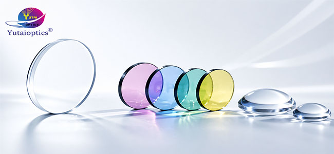
I. Window: Isolates contamination and stabilizes incident light
From an environmental protection perspective, during wafer metrology, contaminants such as photoresist volatiles, fine particles, and water vapor can easily accumulate inside the equipment chamber. If these impurities enter the optical path, they can cause light signal scattering and attenuation, and may even damage the precision optical components downstream. Windows are typically made of high-purity fused quartz, BK7 optical glass, or specialty crystal materials. Their surfaces are coated with anti-reflection (AR) and water- and contamination-repellent coatings, which effectively prevent contaminants from adhering, protect the windows from corrosion, and shield core components such as filters and lenses from damage, ensuring the long-term stable operation of the optical system.
To ensure optical path stability and maintain light flux, the window must possess extremely high surface precision (typically better than λ/10, where λ = 633 nm), parallelism, and low-stress birefringence characteristics. Its double-sided anti-reflective coating reduces light reflectance to below 0.2%, minimizing energy loss in the optical signal to the greatest extent possible. This ensures that incident light transmits perpendicularly without additional deflection and with minimal wavefront distortion, providing a stable and pure incident light signal for downstream filters and lenses. For measurement scenarios involving special wavelength bands such as deep ultraviolet (DUV, 193 nm) and infrared (IR), the window must be made of a material with high transmittance in the corresponding wavelength band, while also possessing a high laser-induced damage threshold (LIDT) and excellent thermal stability. This prevents thermal deformation or component damage under high-energy light sources, meeting the measurement requirements of various manufacturing processes.
II. Filters: Filter out interference and improve the signal-to-noise ratio
In monochromatic light measurement applications (such as laser interferometry and nanoscale topography analysis), narrowband filters play a critical role. Their core parameters include center wavelength (CWL), full width at half maximum (FWHM), peak transmittance, and cutoff depth (OD). For example, in measurements in the 850 nm near-infrared band, the center wavelength error of a narrowband filter must be controlled within ±2 nm, the FWHM must be only 10–20 nm, the peak transmittance must exceed 85%, and the cut-off depth must be OD > 4 (i.e., stray light transmittance < 0.01%). This allows for the precise transmission of the target inspection light while completely blocking interfering signals such as ambient light, stray light from the wafer surface, and light source harmonics. It improves the signal-to-noise ratio of defect detection by more than 10 times, ensuring the accurate identification of minute defects (such as 14-nm-level particles and scratches).
To meet multi-wavelength measurement requirements, the equipment is also equipped with various types of filters, such as short-pass, long-pass, and bandpass filters. For example, in white-light interferometry, a 400–700 nm visible light bandpass filter is used to capture broad-spectrum interferometric signals, enabling precise measurement of film thickness. In silicon wafer line width inspection, a short-pass filter effectively blocks infrared noise generated by wafer heating, preventing noise interference with image quality and ensuring the accuracy of line width measurements. Additionally, filters must exhibit low angle sensitivity (typically <0.5 nm/10°) to ensure stable spectral filtering performance even when the optical path is slightly deflected, thereby supporting multi-mode imaging requirements such as brightfield, darkfield, and confocal imaging.
III. Lenses: Determining Resolution and Imaging Accuracy
High numerical aperture (NA) is one of the core design parameters for lenses. Optical resolution is inversely proportional to the wavelength (λ) of the light source and directly proportional to the numerical aperture. Imaging lenses for advanced process measurement equipment require a numerical aperture of 0.8–0.95. When paired with short-wavelength light sources (such as 193 nm DUV), the theoretical resolution can exceed 30 nm, enabling the stable detection of minute defects and pattern misalignments on the wafer surface, thereby meeting the measurement requirements for 3 nm and smaller processes.
Aberration correction capability is another key advantage of lenses. Wafer metrology requires uniform imaging across a wide spectral range and a large field of view; therefore, imaging lenses typically employ a plan-apochromatic design, consisting of multiple groups of positive and negative elements. By using low-dispersion optical glass (such as fluorite and ultra-low dispersion glass), these lenses can simultaneously correct spherical aberration, comatic aberration, chromatic aberration, and field curvature, ensuring flat imaging across the entire field of view with consistent sharpness and eliminating measurement errors caused by aberrations. Additionally, to further optimize the optical path structure and reduce spherical aberration, lens assemblies often incorporate elements such as plano-convex lenses and positive meniscus lenses: Plano-convex lenses feature a simple structure and lower cost, making them suitable for low-precision collimation applications; Positive meniscus lenses (one convex and one concave, with a thicker center and thinner edges) effectively correct spherical aberration and provide superior imaging clarity compared to plano-convex lenses; they are widely used in high-precision wafer measurement optical paths.
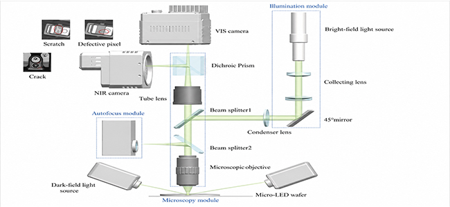
IV. The three components work together to establish a complete optical chain for wafer measurement
In the actual measurement optical path, the window, filter, and imaging lens are arranged in series to form a closed-loop synergy of “protection—filtering—imaging,” supporting multimodal measurement scenarios such as brightfield, darkfield, white-light interferometry, and spectral confocal imaging.
1. Incident phase: The detection light (laser or white light) emitted by the light source first passes through the window, which filters out large particles to ensure that the light signal is free of scattering and energy loss;
2. Filtering stage: Pure incident light reaches the filter, which precisely selects the target wavelength while blocking stray light and noise, resulting in monochromatic light with a high signal-to-noise ratio;
3. Imaging stage: When monochromatic light strikes the wafer surface, it is reflected. The reflected light, which carries information about the surface topography and defects, enters the imaging lens. The lens corrects for aberrations and focuses the light, clearly imaging the nanoscale microstructure onto the sensor, which is then converted into analyzable electrical signals and image data.
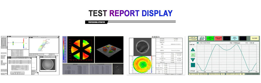
As semiconductor processes advance toward 2nm and 1nm, Yutai Optics leverages its technical expertise and R&D capabilities to focus on optimizing the performance of windows, filters, and lenses. By precisely meeting the stringent requirements of advanced processes for optical components, the company develops highly reliable products tailored to diverse measurement scenarios. This enables efficient synergy among these three key components, thereby enhancing the accuracy and efficiency of wafer measurement equipment.
I. Window: Isolates contamination and stabilizes incident light
From an environmental protection perspective, during wafer metrology, contaminants such as photoresist volatiles, fine particles, and water vapor can easily accumulate inside the equipment chamber. If these impurities enter the optical path, they can cause light signal scattering and attenuation, and may even damage the precision optical components downstream. Windows are typically made of high-purity fused quartz, BK7 optical glass, or specialty crystal materials. Their surfaces are coated with anti-reflection (AR) and water- and contamination-repellent coatings, which effectively prevent contaminants from adhering, protect the windows from corrosion, and shield core components such as filters and lenses from damage, ensuring the long-term stable operation of the optical system.
To ensure optical path stability and maintain light flux, the window must possess extremely high surface precision (typically better than λ/10, where λ = 633 nm), parallelism, and low-stress birefringence characteristics. Its double-sided anti-reflective coating reduces light reflectance to below 0.2%, minimizing energy loss in the optical signal to the greatest extent possible. This ensures that incident light transmits perpendicularly without additional deflection and with minimal wavefront distortion, providing a stable and pure incident light signal for downstream filters and lenses. For measurement scenarios involving special wavelength bands such as deep ultraviolet (DUV, 193 nm) and infrared (IR), the window must be made of a material with high transmittance in the corresponding wavelength band, while also possessing a high laser-induced damage threshold (LIDT) and excellent thermal stability. This prevents thermal deformation or component damage under high-energy light sources, meeting the measurement requirements of various manufacturing processes.
II. Filters: Filter out interference and improve the signal-to-noise ratio
In monochromatic light measurement applications (such as laser interferometry and nanoscale topography analysis), narrowband filters play a critical role. Their core parameters include center wavelength (CWL), full width at half maximum (FWHM), peak transmittance, and cutoff depth (OD). For example, in measurements in the 850 nm near-infrared band, the center wavelength error of a narrowband filter must be controlled within ±2 nm, the FWHM must be only 10–20 nm, the peak transmittance must exceed 85%, and the cut-off depth must be OD > 4 (i.e., stray light transmittance < 0.01%). This allows for the precise transmission of the target inspection light while completely blocking interfering signals such as ambient light, stray light from the wafer surface, and light source harmonics. It improves the signal-to-noise ratio of defect detection by more than 10 times, ensuring the accurate identification of minute defects (such as 14-nm-level particles and scratches).
To meet multi-wavelength measurement requirements, the equipment is also equipped with various types of filters, such as short-pass, long-pass, and bandpass filters. For example, in white-light interferometry, a 400–700 nm visible light bandpass filter is used to capture broad-spectrum interferometric signals, enabling precise measurement of film thickness. In silicon wafer line width inspection, a short-pass filter effectively blocks infrared noise generated by wafer heating, preventing noise interference with image quality and ensuring the accuracy of line width measurements. Additionally, filters must exhibit low angle sensitivity (typically <0.5 nm/10°) to ensure stable spectral filtering performance even when the optical path is slightly deflected, thereby supporting multi-mode imaging requirements such as brightfield, darkfield, and confocal imaging.
III. Lenses: Determining Resolution and Imaging Accuracy
High numerical aperture (NA) is one of the core design parameters for lenses. Optical resolution is inversely proportional to the wavelength (λ) of the light source and directly proportional to the numerical aperture. Imaging lenses for advanced process measurement equipment require a numerical aperture of 0.8–0.95. When paired with short-wavelength light sources (such as 193 nm DUV), the theoretical resolution can exceed 30 nm, enabling the stable detection of minute defects and pattern misalignments on the wafer surface, thereby meeting the measurement requirements for 3 nm and smaller processes.
Aberration correction capability is another key advantage of lenses. Wafer metrology requires uniform imaging across a wide spectral range and a large field of view; therefore, imaging lenses typically employ a plan-apochromatic design, consisting of multiple groups of positive and negative elements. By using low-dispersion optical glass (such as fluorite and ultra-low dispersion glass), these lenses can simultaneously correct spherical aberration, comatic aberration, chromatic aberration, and field curvature, ensuring flat imaging across the entire field of view with consistent sharpness and eliminating measurement errors caused by aberrations. Additionally, to further optimize the optical path structure and reduce spherical aberration, lens assemblies often incorporate elements such as plano-convex lenses and positive meniscus lenses: Plano-convex lenses feature a simple structure and lower cost, making them suitable for low-precision collimation applications; Positive meniscus lenses (one convex and one concave, with a thicker center and thinner edges) effectively correct spherical aberration and provide superior imaging clarity compared to plano-convex lenses; they are widely used in high-precision wafer measurement optical paths.
IV. The three components work together to establish a complete optical chain for wafer measurement
In the actual measurement optical path, the window, filter, and imaging lens are arranged in series to form a closed-loop synergy of “protection—filtering—imaging,” supporting multimodal measurement scenarios such as brightfield, darkfield, white-light interferometry, and spectral confocal imaging.
1. Incident phase: The detection light (laser or white light) emitted by the light source first passes through the window, which filters out large particles to ensure that the light signal is free of scattering and energy loss;
2. Filtering stage: Pure incident light reaches the filter, which precisely selects the target wavelength while blocking stray light and noise, resulting in monochromatic light with a high signal-to-noise ratio;
3. Imaging stage: When monochromatic light strikes the wafer surface, it is reflected. The reflected light, which carries information about the surface topography and defects, enters the imaging lens. The lens corrects for aberrations and focuses the light, clearly imaging the nanoscale microstructure onto the sensor, which is then converted into analyzable electrical signals and image data.
As semiconductor processes advance toward 2nm and 1nm, Yutai Optics leverages its technical expertise and R&D capabilities to focus on optimizing the performance of windows, filters, and lenses. By precisely meeting the stringent requirements of advanced processes for optical components, the company develops highly reliable products tailored to diverse measurement scenarios. This enables efficient synergy among these three key components, thereby enhancing the accuracy and efficiency of wafer measurement equipment.
Share this:
PREV : Good cutting = high-power laser + high-performance window NEXT : Changchun Yutai Optics has officially moved into the Automotive Innovation Park, Liando U Valley
TALK TO US 86-15584132290
Call us now!
86-15584132290Call us now!

ONLINE CHAT
 2433808388